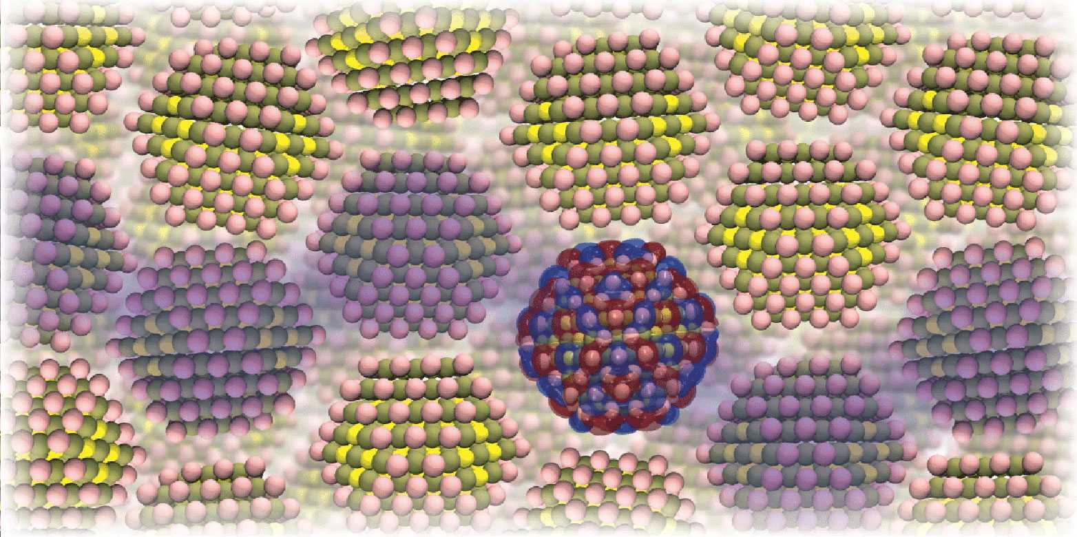
A new theory for Semiconductors made of nanocrystals
Researchers at ETH have provided the first theoretical explanation for how electrical current is conducted in semiconductors made of nanocrystals. In the future, this could lead to the development of new sensors, lasers or LEDs for TV screens.
A few years ago, we were introduced to TV screens featuring QLED technology that produces brilliant colours. The “Q” here stands for “quantum dot”. Quantum dots are crystals of a semiconductor material only a few nanometres in size that consist of a couple of thousand atoms. Those nanocrystals are so tiny that the electrons in them can only take on certain well-defined quantum mechanical energy levels. As a consequence, when quantum dots are illuminated by the backlight of a TV, light of a particular colour is emitted by quantum jumps between those levels.
Read the full article featuring Vanessa Wood and Nuri Yazdani in ETH News.
See our research lab.
