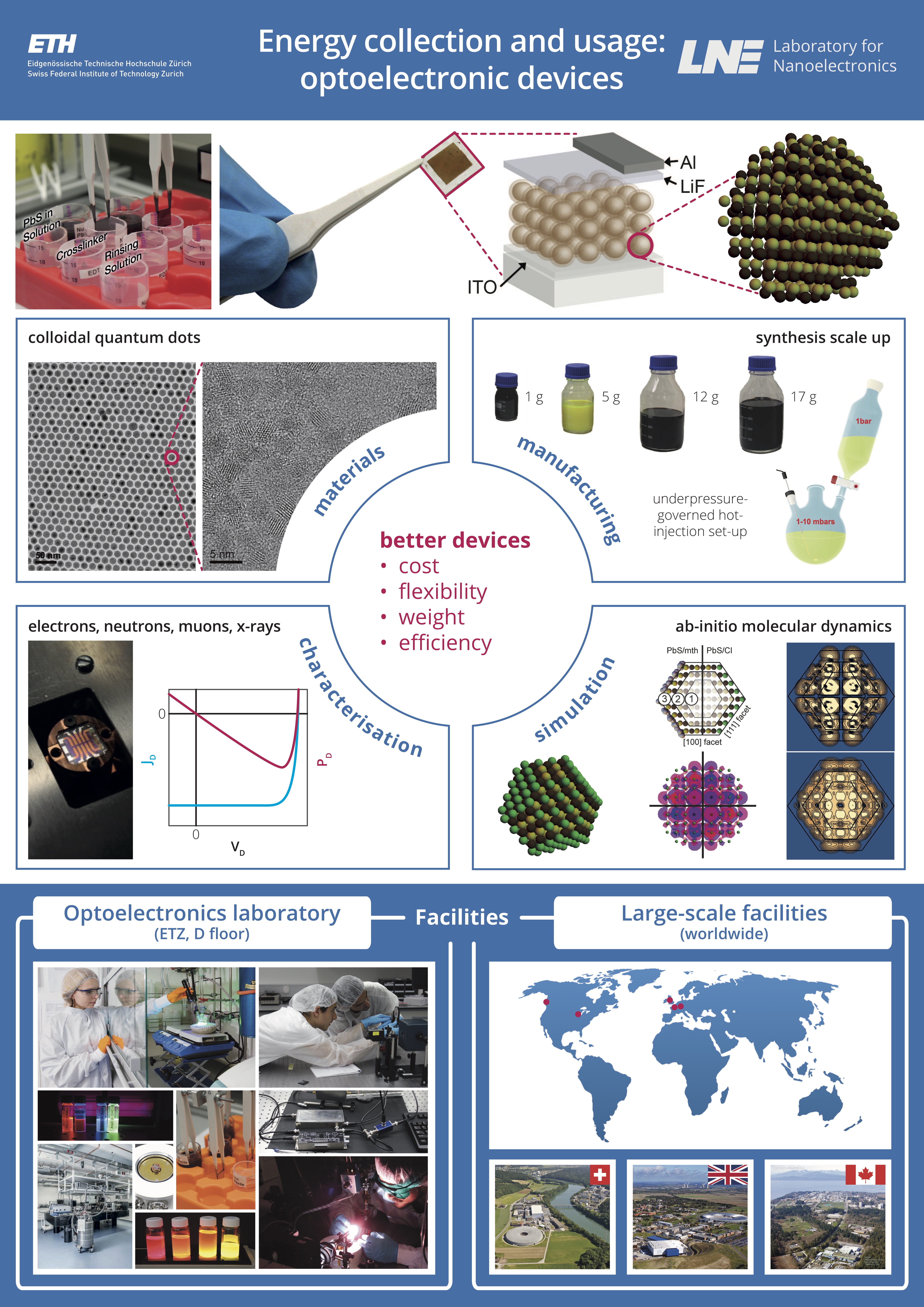
(Opto)electronics Laboratory
(Opto)electronics Laboratory
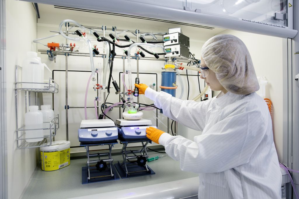
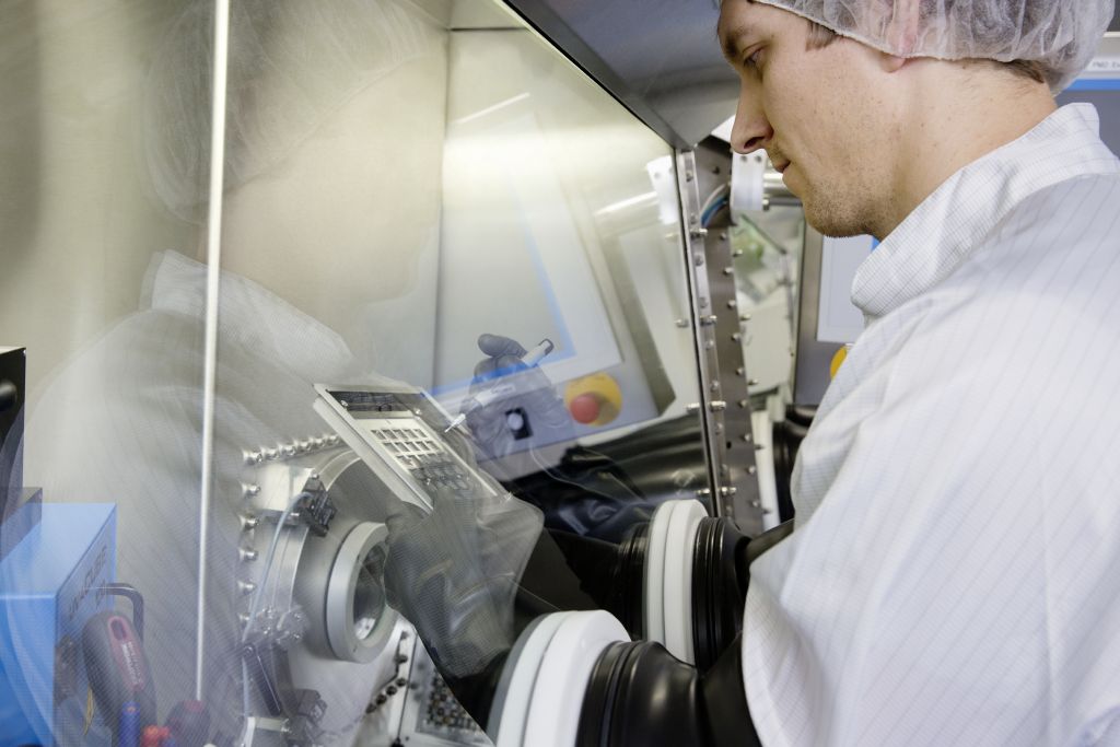
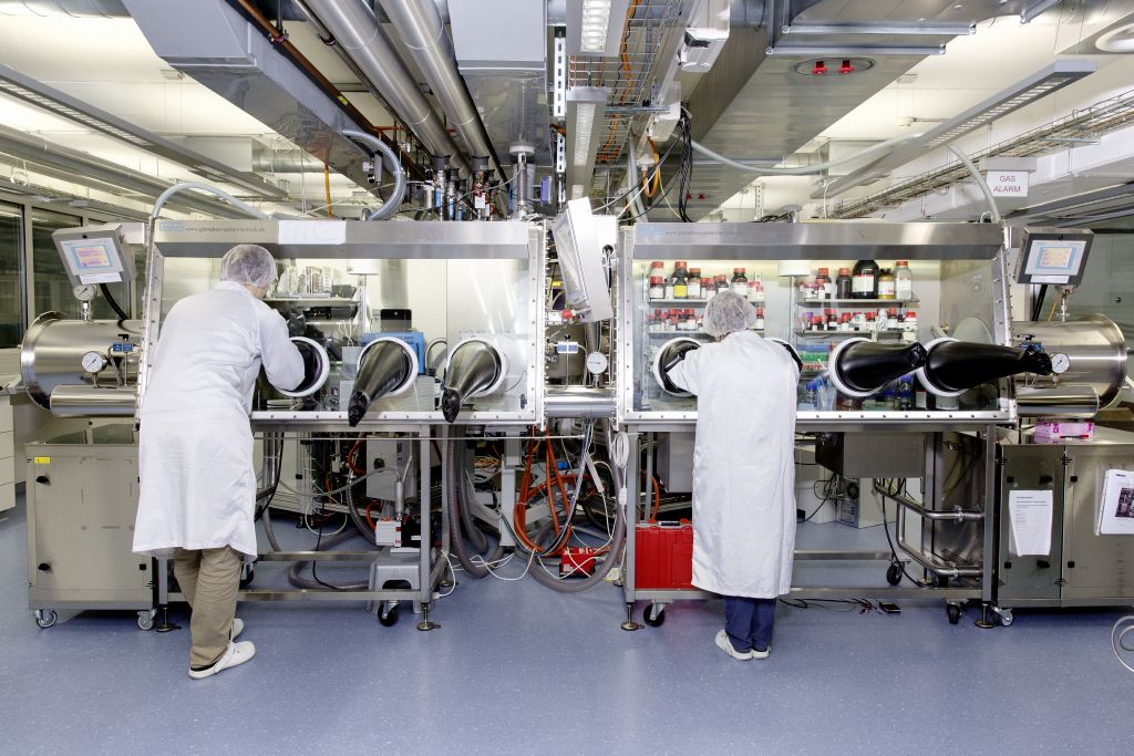
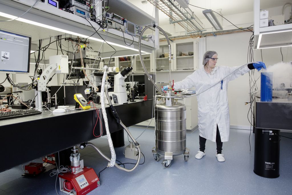
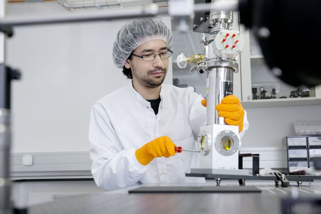
The Materials and Device Engineering Group has two locations. Activities related to optoelectronic materials and devices predominately take place in the ETZ building on the ETH Zürich Zentrum Campus located in downtown Zürich.